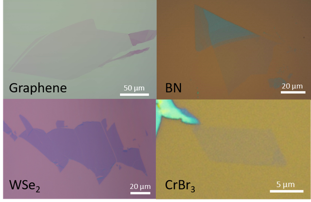
Two-dimensional materials are actually a big family, containing metal, semiconductor, insulator, topological insulator, superconductor, magnet, etc. Theoretical predication suggests there are over 1000 kinds of 2D materials, which can be easily exfoliated [1]. The above optical images show the representative 2D materials. Graphene is the first discovery of 2D materials [2]. The Dirac fermions and high mobility properties make graphene still be the most popular 2D materials even after 15 years from its discovery. Hexagonal-BN is an idea 2D insulator [3], which can simultaneously serve as atomically flat substrate, protecting layer, gate dielectric and tunneling barrier. Monolayer transition metal dichalcogenides, such as WSe2, MoS2, have direct bandgap and inversion symmetry breaking, making them as idea candidates for the study of optoelectronics and valleytronics [4]. Two-dimensional ferromagnets, such as CrBr3 [5], provide the possibility to manipulate spin degree of freedom in 2D system.
During the exfoliation, the main task is to get large area flakes. If the pristine flakes are large enough, there are much more chances to find bubble-free area in the final heterostructures, which is necessary for high-quality device. On the other hand, the large flake is essential for some characterization technique, such as ARPES. Morever, the large device can contribute to the observation of novel quantum effects, such as magnetophonon oscillations in graphene [6].
References:
[1]. N. Mounet, et. al., “Two-dimensional materials from high-throughput computational exfoliation of experimentally known compounds”, Nature Nanotechnology, 13, 246-252, (2018).
[2]. K.S. Novoselov, et. al., “Electric field effect in atomically thin carbon films”, Science, 306(5696), 666-669, (2004).
[3]. C.R. Dean, et. al., “Boron nitride substrates for high-quality graphene electronics”, Nature Nanotechnology, 5, 722-726, (2010).
[4]. K.F. Mak, et. al., “Atomically thin MoS2: a new direct-gap semiconductor”, Physical Review Letters, 105, 136805, (2010).
[5]. M. Kim, et. al., “Micromagnetometry of two-dimensional ferromagnets”, Nature Electronics, 2, 457-463, (2019).
[6]. P. Kumaravadivel, et. al., “Strong magnetophonon oscillatins in extra-large graphene”, Nature Communications, 10, 3334, (2019).